BOM Analyzer
Automotive
Computer Vision
BOM Analyzer is a low-cost reverse engineering tool that takes a series of high-resolution images of a PCB, and even measures the height of components with a line laser that's projected onto the PCB at an angle.
Using a custom computer vision model we achieve 98% accuracy in identifying surface mount components on the PCB. For the remaining 2%, there is a built-in labeling & retraining workflow.
We developed the hardware, control software, classification model, and user interface for this project for an automotive customer from scratch in only a few weeks. Motius is now looking for further pilot customers.
Sensors
The machine uses a single camera to capture close up images of the PCB. Stitching several close-up captures together, avoids tall components occluding parts of the PCB.
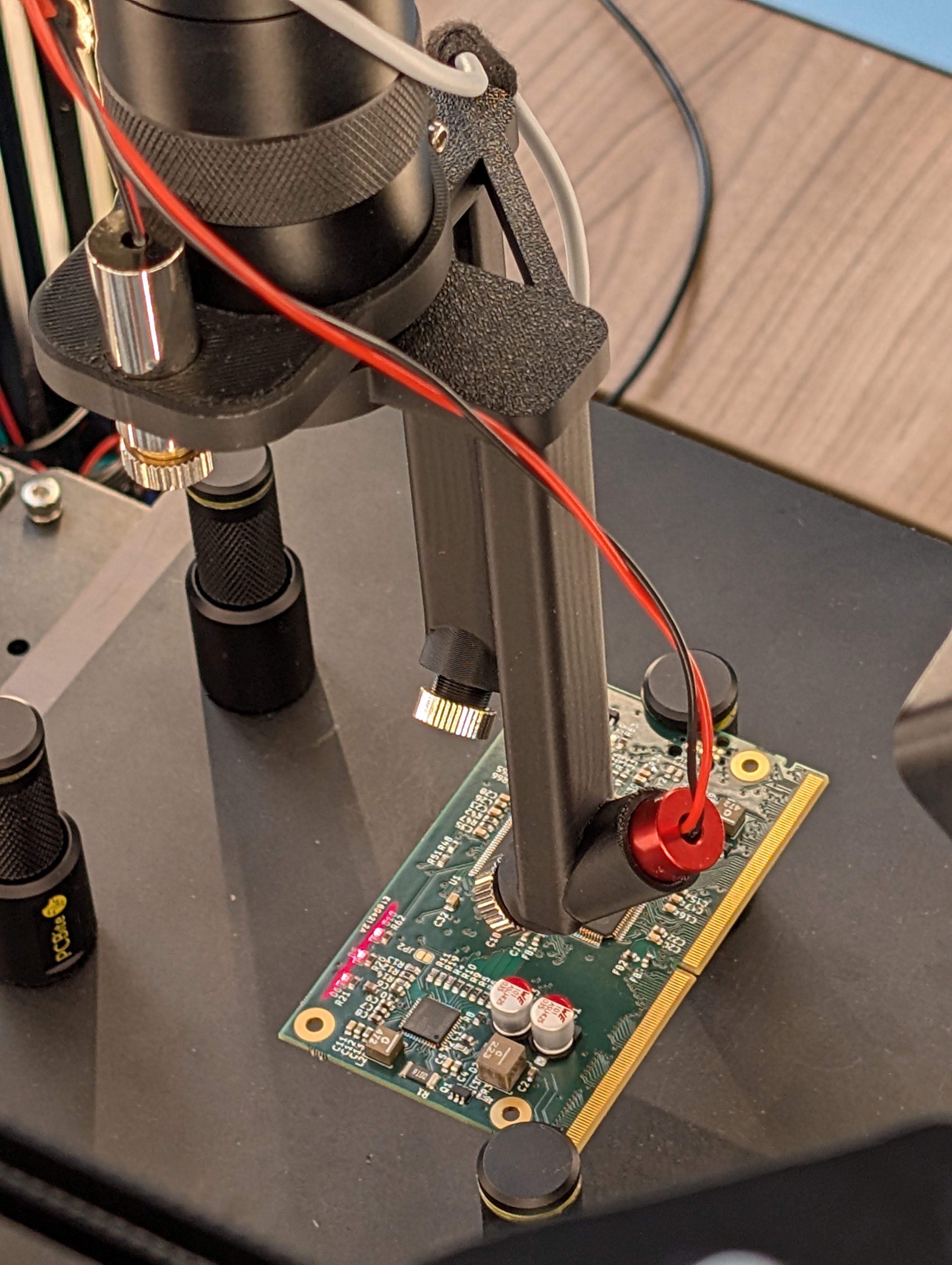
Line laser is visible in the lower left corner of the PCB

One of the red lasers (for height measurement) and green laser (for alignment) turned on. A combination of both are used for the auto focusing the camera
Three lasers are further used for aligning the PCB properly on the scanning bed, for focussing the camera and measuring the height of the components. Two red lasers are used to determine the height of components based on the laser triangulation principle. A combination of both the red and green laser is used for auto-focusing the camera.
Hardware Package
BOM Analyzer is based on an extensible CoreXY design, which can be extended to cover parts of over 1m x 1m, and extremely tall electronic components.

BOM Analyzer is based on a modified CoreXY gantry, image classification can run on an edge device (or in this case on a laptop)
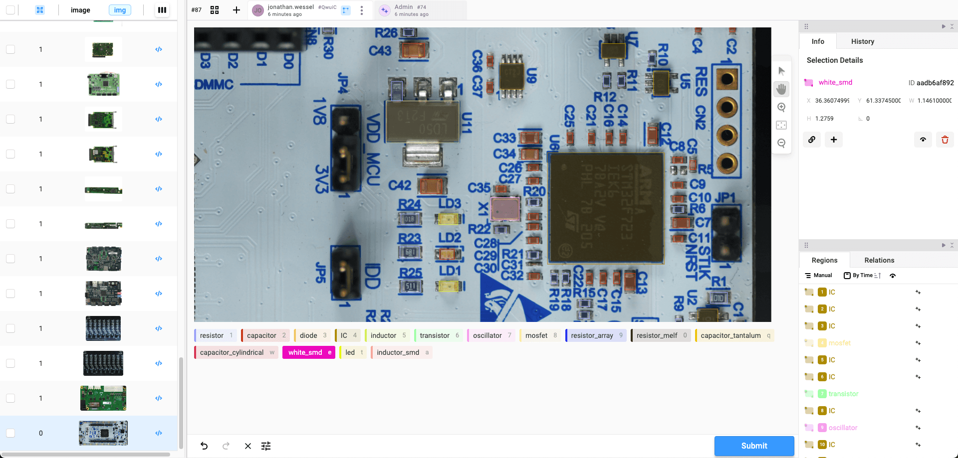
Control Software and User Interface
Our software is easy to use, but still lets experts manually control every aspect of the machine, and dive into every detail of the captured images, classification labels, dimensions, and detected component labels.

Simple user interface, where the user places and aligns the PCB, before starting the scan
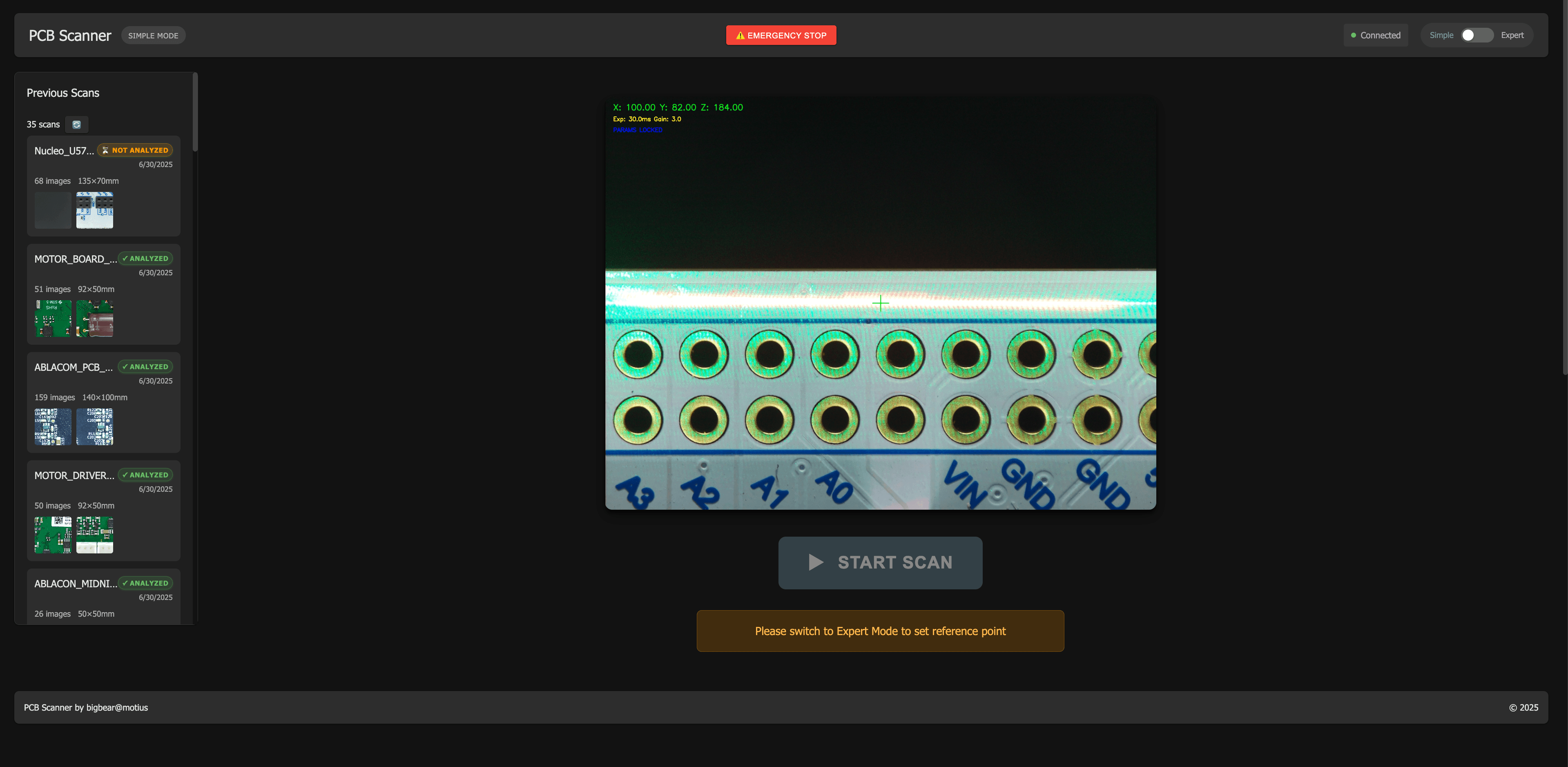
Expert user interface, with more granulare controls and options for the scan
Labeling
Our system is based on a open source foundational model that is trained on open data sets, and then further extended with our own training set. Labeling is done using Label Studio.
Label Studio interface for labelling self scanned data
Results
The result of this design is a low-cost machine that can create highly detailed captures of the larges PCBs in minutes, and analyze & label their components in seconds.
Additionally, we put together our own database of >350,000 components that you will also gain full access to.
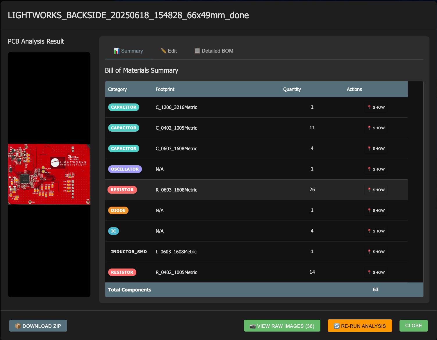
Summary output of the scan, here highlighting the 26 detected reistors

Detailed BOM of the scan, with marking code detection using OCR. This can be used in combination with the marking code database to find components.